
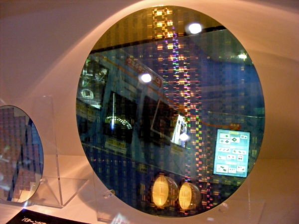
Nanofabrication Tools: Etching and thin films
Subject
Chemistry
Education Level
High School
This is a four-part lesson designed to help students understand the terminology, procedures, and equipment used to manufacture micro and nanoscale products. It helps them explore the processes used in nanofabrication including electroplating, PCB etching and etch time. In this lesson, students will learn basic ways of transferring pattern to build these devices and design a membrane with specific requirements. The lesson ends with a design challenge using information gained in the first three activities. A pre-lab is recommended as either a homework assignment or as an in-class activity. Students will either view a video or read about the fabrication process used in semiconductor manufacturing.